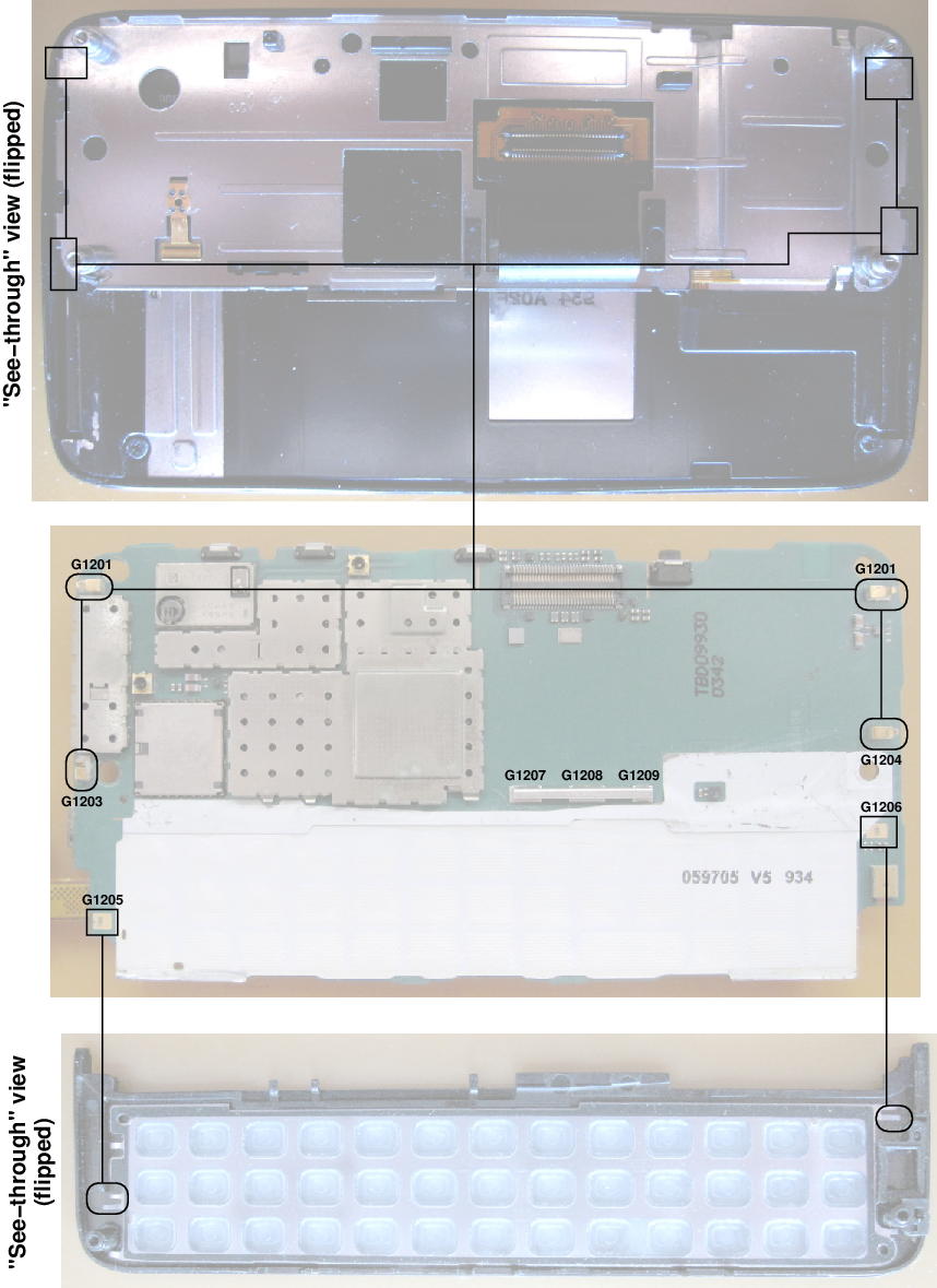
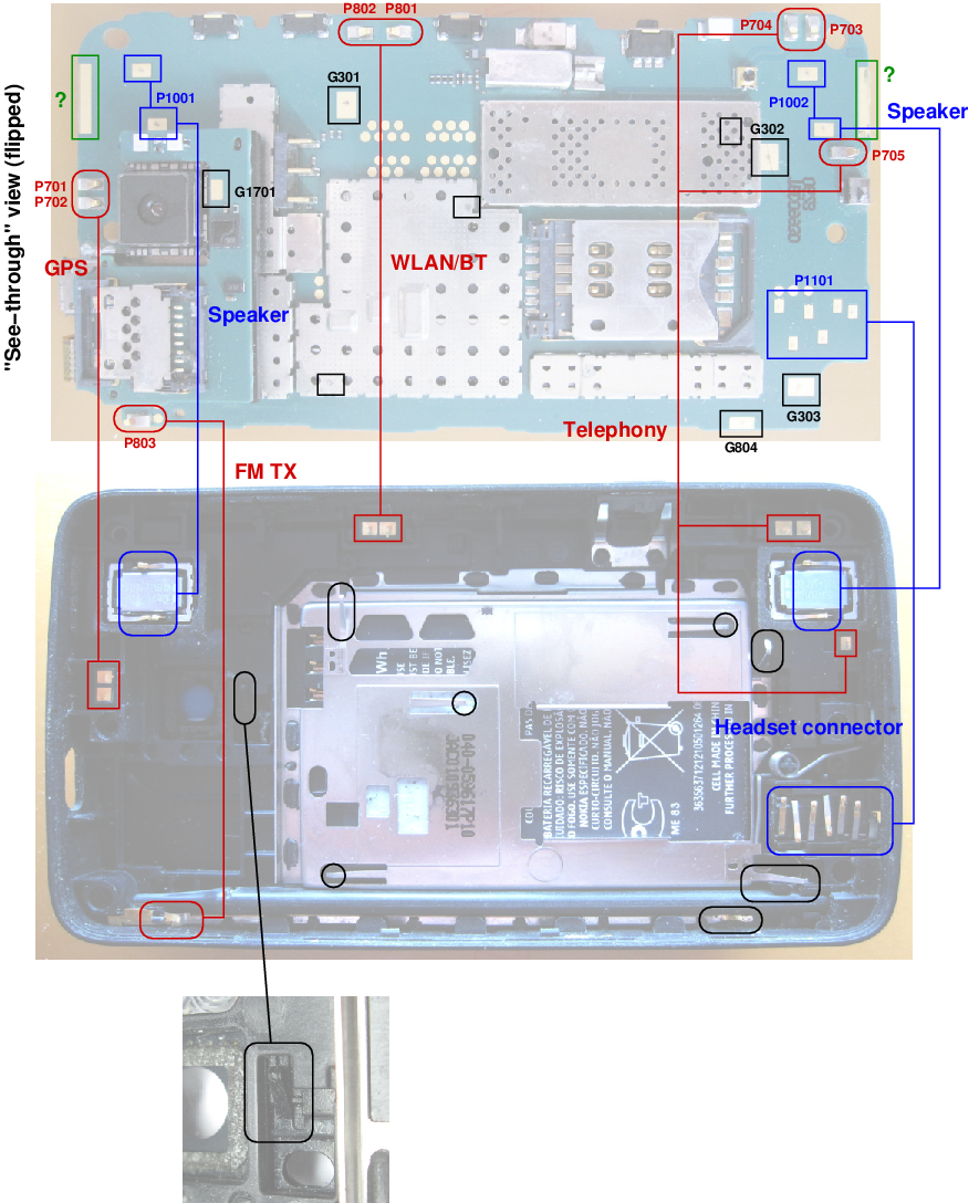
Neo900 Spring-Type Contacts
The following images show where spring-type contacts are located in the
N900, and what role they play. On the PCB, these contacts are either C
springs or just contact pads touched by a spring-like protrusion of a
component located in a mating part.
Since Neo900 interfaces with the same parts (from the original N900
design), it has to provide the same contacts.
We use the following color coding to indicate different types of signals:
- Black indicates contacts that connect shields and similar metal
parts to ground.
- Blue indicates audio connections.
- Red indicates antenna connections.
- Green marks contacts that do not seem to have a peer.
Springs are indicated by rounded rectangles or circles, the location
where they touch (e.g., pad, shield, or similar) by a regular rectangle.
Where it serves clarity, we link groups of mating contacts with a line.
The following images show the respective surfaces as they would appear
when viewing the assembled device from the top with "x-ray vision".
To this end, some images have been flipped (mirrored) along the Y axis.
This also corresponds to the orientation of the PCB surfaces in the
layout editor.
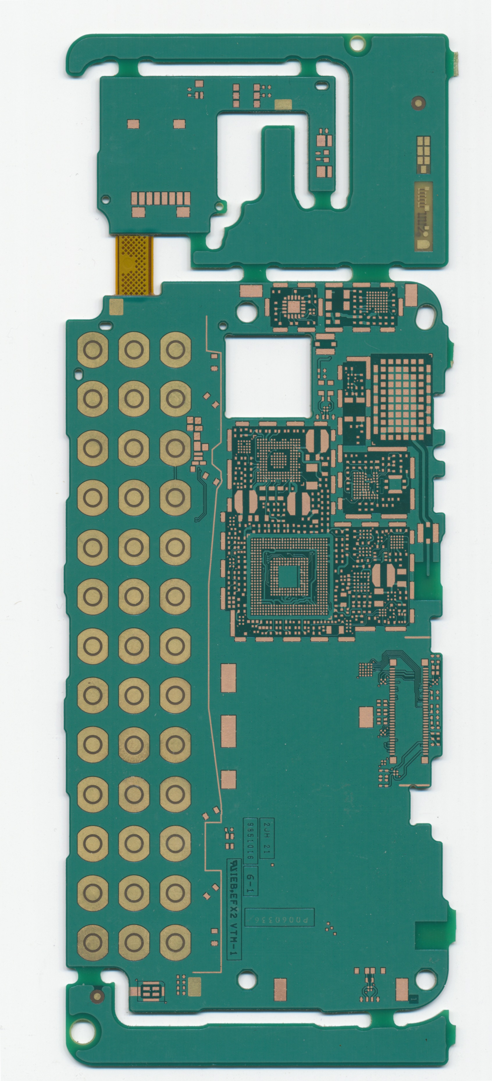
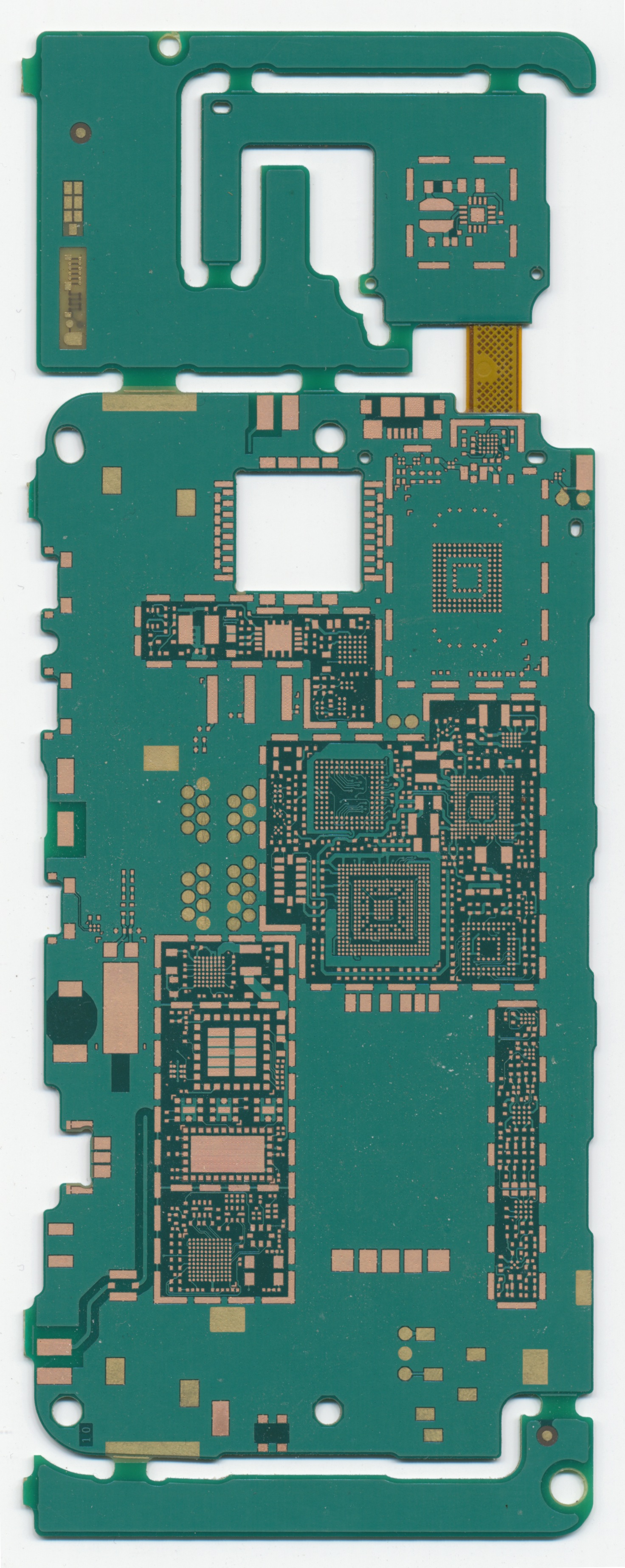
Complementary information: high resolution scans of PCB
top
and
bottom
(for measuring pad dimensions and locations).
PCB top
The PCB top interfaces with the key mat and the display/slider assembly:
PCB bottom
The PCB bottom interfaces with the case and various components contained
therein:
2016-11-22 00:59:10 UTC