In the screenshots below, the mesh is shown in grey, with darkness indicating depth. Where the contrast is increased to better show fine structures, parts of the mesh exceeding the available range of grey tones are shown as yellow. Blue lines at the bottom and the right side are sometimes added to show the height profile along the axes of the cursor (red).
Sections:
All dimensions are in millimeters. The following sections explain how the
measurements used in this drawing were obtained.
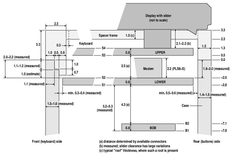
The result is that the case edge is typically between 1.9 to 2.0 mm above
the PCB surface.
The case edge is typically about 2.0-2.2 mm above the PCB surface. The
"step" on which the keyboard frame rests has a depth of about 1.1 to 1.2 mm
and is thus roughly 1 mm above the PCB.
The measurements are between opposite points where the sensed height
markedly falls off, and suggest a thickness of 1.4-1.5 mm. Given that the
top of the wall is slightly curved, which can cause a drop to appear in
the scan before the wall falls off in reality, some measurements are
likely to be too short by up to one grid step (0.1 mm). We therefore
consider the nominal wall thickness to be 1.5 mm.
The result is that the clearance varies considerably but is never smaller
than 0.5 mm.
We obtain an overall wall thickness of 1.5 to 1.6 mm, and a "step"
width of 0.4 to 0.5 mm. The PCB is closer to the wall than on the
rear side, only 0.3 to 0.4 mm.
The first 0.5 to 0.6 mm below top of the case wall are unobstructed.
Then the IR window begins, followed by the volume button with a peak
at about 0.75 mm and the rest at 1.3 mm,
and the camera button at about 0.9 mm.
The middle "hook" seems to be centered at the middle of the case. Most
of these measurements are between edges that not perpendicular to the
measurement direction and sometimes even rounded, and may therefore be
fairly inexact.
The general observation is that that basic shape of this metal structure
is a plane with some cut-outs into which shallow details have been
stamped, and from which larger structures protrude. We can therefore
measure all heights relative to this plane.
The following different features are being measured here:
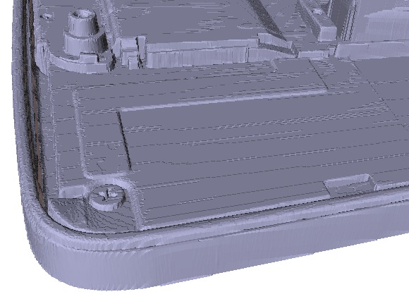
At this location, the spacer is not in contact with the PCB directly,
but rests on the light spreader, which has a thickness of about 150 μm.
One can also see that the spacer has compressed the light spreader by
about 50 μm.
These measurements show a systematic difference to the wall thickness of
1.5 mm. This can be explained by the shape of the display case, which
transitions from the plateau to the wall through a small step. This step
is almost invisible in the mesh at the top edge but can be clearly seen
at the bottom edge:
With the scanning equipment equipment used, such a step is difficult to
measure accurately due to the conical shape of the scanning needle.
Combining results from the top and the bottom
edge (below), we estimate the step to have a width of about 0.4±0.1 mm.
We show distances corrected for the step width in parentheses after the
original measurement. The minimum distance between slider metal and the
case is thus 0.1 mm, with the gap sometimes growing to about 0.5 mm (zones A
a and B) or even 0.8 mm (zone C).
The measurements also show a significant difference between the distance
between slider and the outside wall of the display on the left and on the
right side. We did not examine this further, but consider it possible that
the difference may have been caused the 0.4 mm step entering some of the
measurement while being absent from the others.
Note that, while the scan shows a clearly visible rotation in the XY
plane, its effect on measurements is negligible. (E.g., the real
distance between the two columns is only about 0.02% larger than its
X distance.)
2016-10-26 23:39:12 UTC
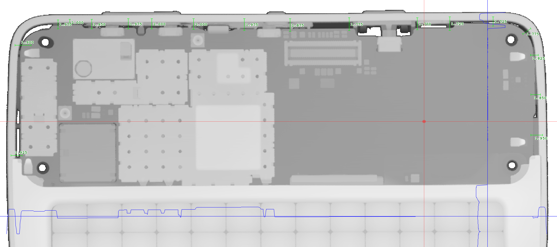
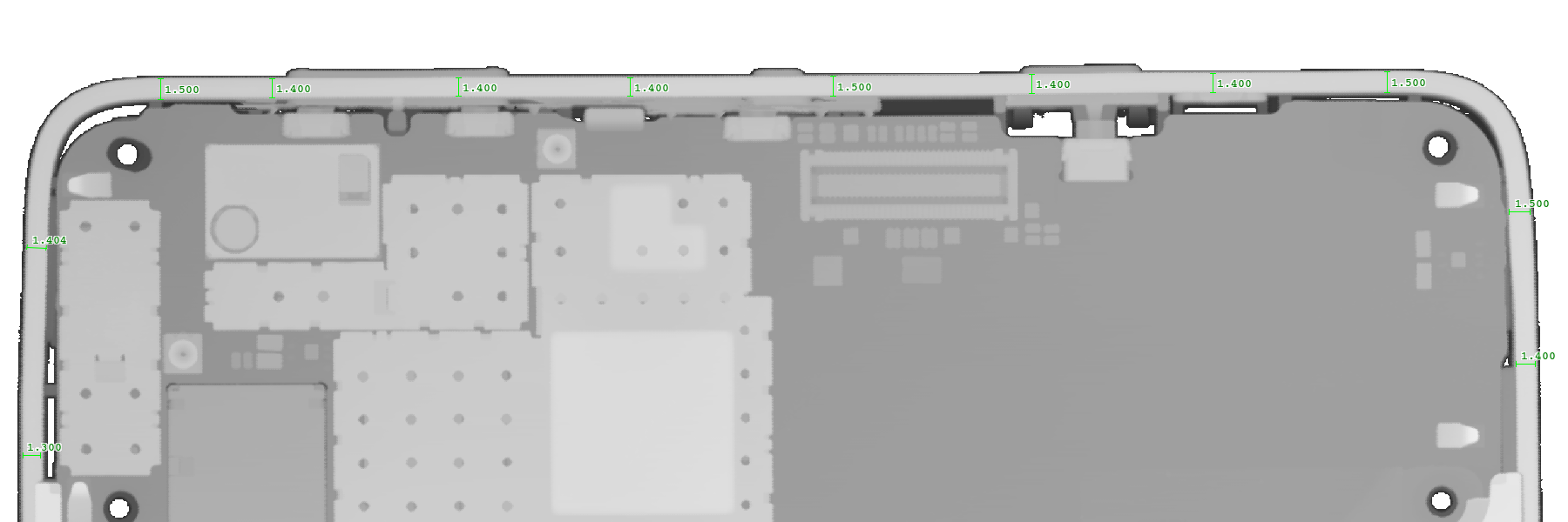
Case edge height (rear side)
The following set of measurements shows the height of the case edge over
the top surface (S2) of the PCB. The green measurements lines indicate
the pairs of points whose Z difference is being measured.
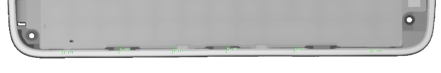
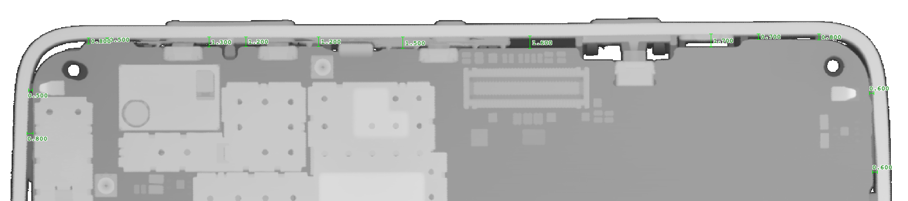
Case edge height (front side)
We repeat the same measurements on the front (keyboard) side.
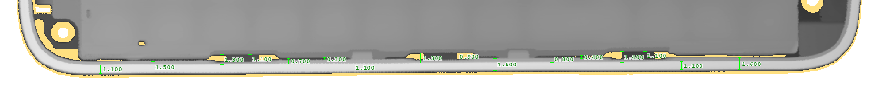
Case wall thickness (rear side)
For designing the side walls of the spacer frame and for calculating
clearances (in the next section), we need to know the thickness of the
case wall.
PCB to case clearance (rear side)
This set of measurements shows the horizontal clearance between the
PCB (LOWER) and the case. The green measurement lines show the distances
being measured.
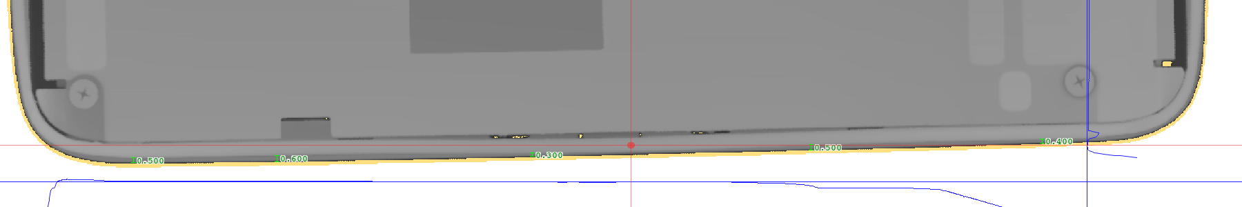
PCB to case clearance and wall thickness (front side)
This set of measurements shows the horizontal clearance between the
PCB (LOWER) and the front side of the case, and it also shows the
thickness of the wall.
The green measurement lines indicate the distances being measured.
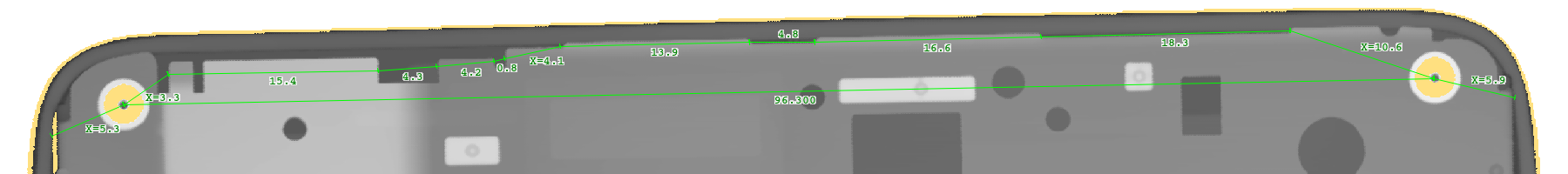
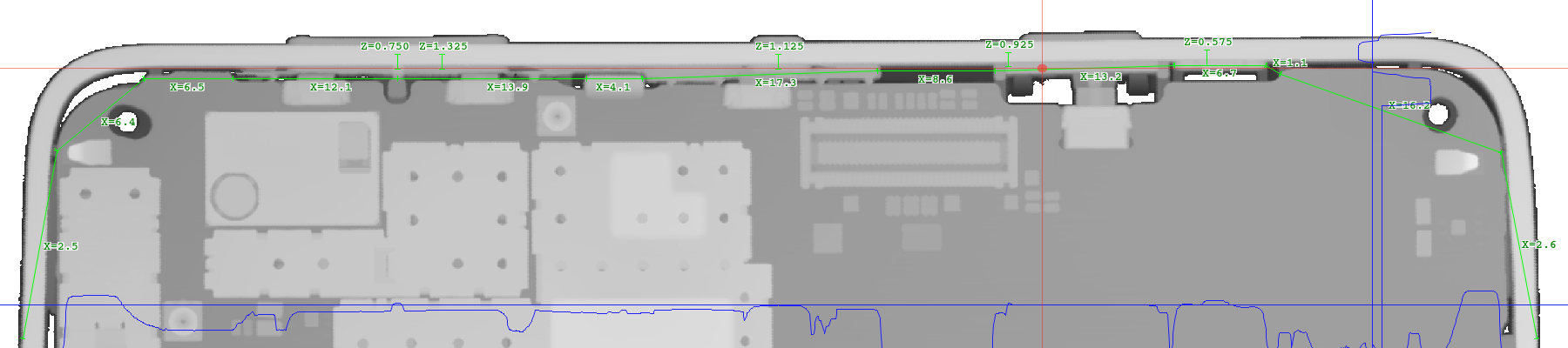
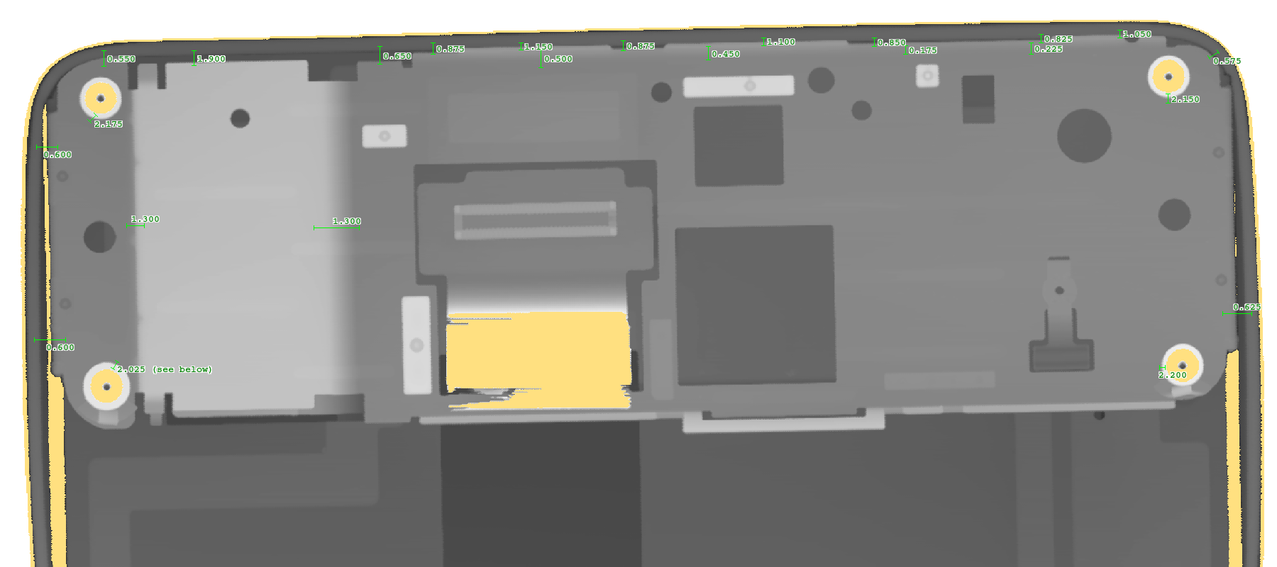
Location of rear (button) side features, vertical clearance near wall
This set of measurements show there where features on the rear side
are placed along the X axis. It also indicates the vertical distance
between the top of the case wall and the most prominent rear-side features.
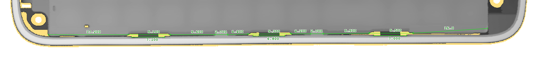
Location of front (keyboard) side features
The following set of measurements shows where features on the front side
are placed along the X axis:
Vertical structure of the slider
The height (or depth) of details of the metal structure of the slider
mechanism is examined in the following set of measurements. Special
attention is given to the height of the bends at the upper end of the
slider. The measurement
lines indicate the points whose heights are being compared.
We obtain a value of 2.1-2.2 mm, with an important outlier of only
2.0 mm in the bottom left corner. This is further examined in a
separate set of measurements, below.
Spacer on light spreader
The outlier observed above can be explained by closer examination of where
the spacer touches the PCB. The following image zooms into the
PCB-with-case scan we have used before, showing the lower right corner,
right above the keyboard:
![]()
Slider to case clearance
In order to explore possibilities for adding stabilizing elements to the
spacer frame, we need to determine the horizontal gap between case and
slider mechanism. We measure this indirectly by determining the distance
between the steep outer side of the display and the edge of the slider.
Using the case wall thickness, the gap between slider and wall can then
be calculated.
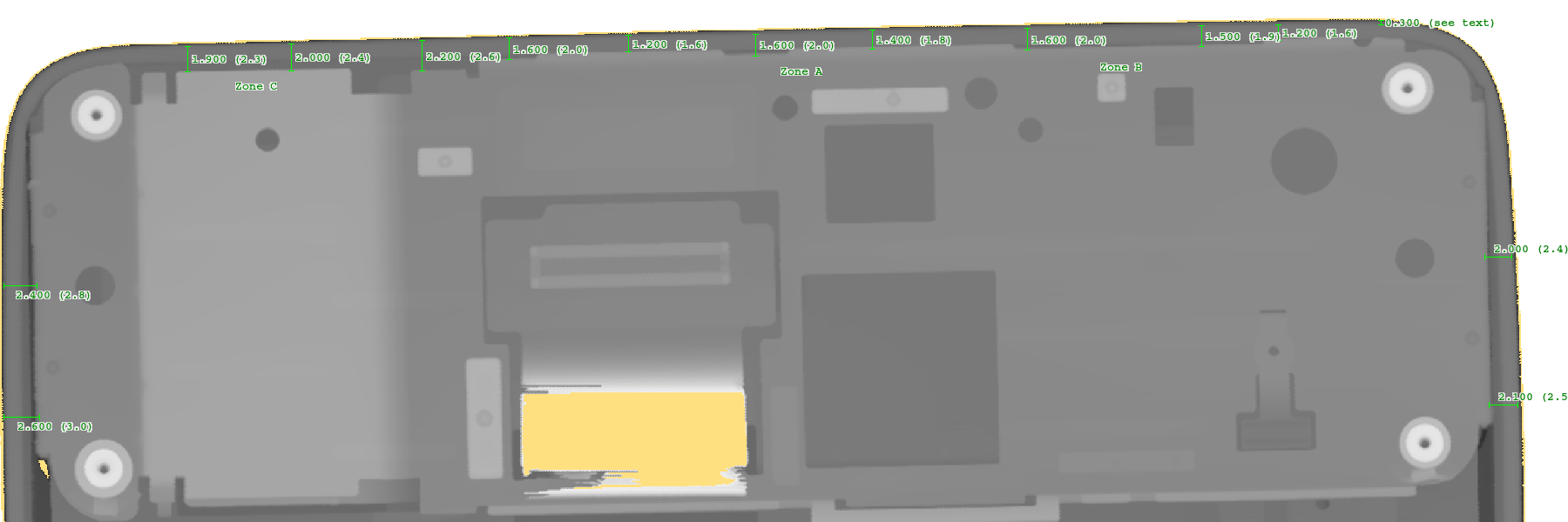
Location of slider features
The following set of measurements shows where features on the slider are
are located along the X axis. While some measurements were made between
points that also differ in the Y direction, we only use the X difference.